

A Gerber file is a vector-based 2D image format that tells printed circuit board (PCB) manufacturers how to fabricate each layer of a board. The Gerber format stores copper trace layouts, solder mask openings, and silkscreen markings in plain ASCII (American Standard Code for Information Interchange) text. Drill data travels in a separate Excellon file. All major electronic design automation (EDA) tools export Gerber data. PCB fabrication facilities worldwide accept the format.
Ucamco owns the Gerber specification and maintains it from Ghent, Belgium. The company calls the format “the backbone of the electronics fabrication industry.” RS-274X (Extended Gerber) is the current standard. RS-274X supports embedded aperture definitions, metadata attributes, and coordinates precisely down to 1 nm. The Gerber format enables accurate PCB fabrication by translating design intent into machine-readable instructions.
The Origin and Evolution of Gerber Files
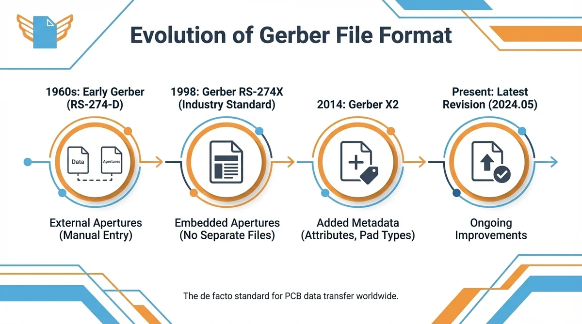
Gerber Scientific Instrument Company created the Gerber format in the 1960s for vector photoplotters. A photoplotter is a precision machine that uses a focused light beam to expose film. The exposed film becomes the artwork for manufacturing copper layers on printed circuit boards. Modern PCB production has largely replaced photoplotters with direct imaging technology, but the Gerber file format itself persists.
The original command set followed the EIA (Electronic Industries Alliance) RS-274-D specification. RS-274-D was a general numerical control (NC) format for NC machines. Gerber Scientific adapted a subset for photoplotter use. The format had a serious flaw: aperture definitions lived in a separate file. Engineers typed aperture codes by hand, and manual entry often ruined production runs.
In April 1998, Barco ETS acquired Gerber Systems Corporation and later became Ucamco. Ucamco published the Gerber Layer Format Specification in September 1998. RS-274X replaced the older RS-274D format family and became the de facto industry standard for Gerber data.
The format passed through several major milestones after that initial release:
- RS-274X embedded aperture definitions inside each file. That change removed the need for separate aperture lists.
- Ucamco reviewed 10,000 Gerber files worldwide in 2012. The review deprecated rarely used constructs.
- Ucamco released Gerber X2 in February 2014. X2 added metadata attributes for file functions and pad types.
- Ucamco declared RS-274-D obsolete on May 30, 2014. Formal revocation followed in September 2014.
- The latest specification, Revision 2024.05, continues to improve the format.
The Gerber format remains the de facto standard for PCB data transfer worldwide.
Gerber File Fundamentals
Understanding what a Gerber file is in PCB design starts with its purpose. A Gerber file is the fabrication instruction for each layer of a printed circuit board. EDA software such as Altium Designer, KiCad, and Autodesk Fusion 360 offers component libraries and generates Gerber output after a designer completes the board layout. These tools also run design rule checking (DRC) before export to verify trace widths, clearances, and pad sizes.
A schematic design describes the circuit logic, component placement, and electrical connections of a board. The schematic captures design intent at a functional level and supports verification through simulation and analysis. A printed circuit board implements that schematic as a physical object.
Gerber files contain layer information for copper traces, solder mask openings, silkscreen markings, and drill holes. Each layer type requires a separate Gerber file. PCB manufacturers use these files to produce finished printed circuit boards with precision.
The Data Structure of a Gerber File
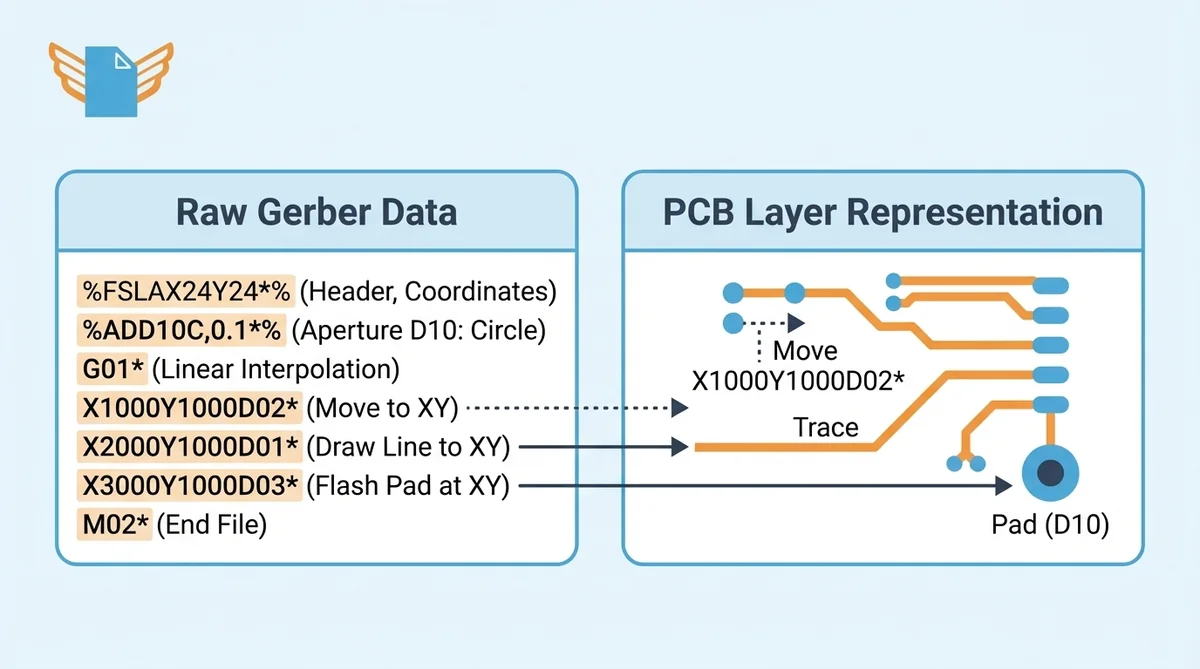
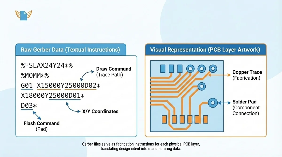
The Gerber file structure follows a simple, readable pattern. Each .gbr file is a plain-text ASCII document with a stream of drawing commands. The Gerber format specification defines the complete command language using just 27 total commands. Each command carries layer information that maps directly to a physical PCB feature.
The file begins with a header declaring coordinate format and unit settings. A typical format statement looks like %FSLAX24Y24*%. That code specifies leading-zero suppression, absolute coordinates, and a 2.4 decimal format.
After the header, aperture definitions describe the shapes used for drawing. D-codes (D10, D11, D12) assign identifiers to aperture shapes: circles, rectangles, and ovals. Specific D-codes represent copper pads, solder mask openings, and silkscreen features. The main body contains G-codes and coordinate commands:
- G01 activates linear interpolation for straight traces between XY coordinates
- G02 and G03 control clockwise and counterclockwise arc interpolation
- D01 draws from the current position to the specified coordinate
- D02 moves the tool head without drawing
- D03 flashes the current aperture at the XY location to create pads and vias
An M02 command ends the file and signals the close of the data stream. Engineers can manually edit Gerber data when troubleshooting problems, because the format uses printable 7-bit ASCII characters.
Gerber File Formats Explained: RS-274D, RS-274X, and X2
Three major Gerber format versions have shaped PCB manufacturing. Each version addressed limitations of its predecessor.
| Feature | RS-274D | RS-274X | Gerber X2 |
|---|---|---|---|
| Aperture definitions | External file | Embedded in file | Embedded in file |
| Metadata support | None | None | File function, pad type, net names |
| Coordinate precision | Limited | Up to 1 nm | Up to 1 nm |
| Status (2026) | Revoked in 2014 | Active, widely used | Active, recommended |
| EDA support | Rarely offered | Universal | Growing adoption |
RS-274D required a separate aperture wheel file. Any mismatch produced fabrication errors. Less than 2% of PCB jobs still use the Standard Gerber file format, according to Ucamco.
RS-274X solved the aperture problem by embedding shape definitions directly into each file. The Extended Gerber format achieved universal support across EDA tools and fabrication houses.
Gerber X2 extends RS-274X with four attribute commands: TF, TA, TO, and TD. These attributes tell the fabricator whether a file is top copper, bottom solder mask, or another layer. The X2 format maintains full backward compatibility with X1 readers.
ODB++, developed by Valor Computerized Systems (later acquired by Mentor Graphics, now Siemens), offers an alternative that packages all layers into a single database file. IPC-2581, maintained by the IPC standards organization, provides a similar all-in-one approach with XML-based data exchange. Neither format has displaced Gerber due to higher complexity and narrower tool support.
What Does a Gerber File Look Like?
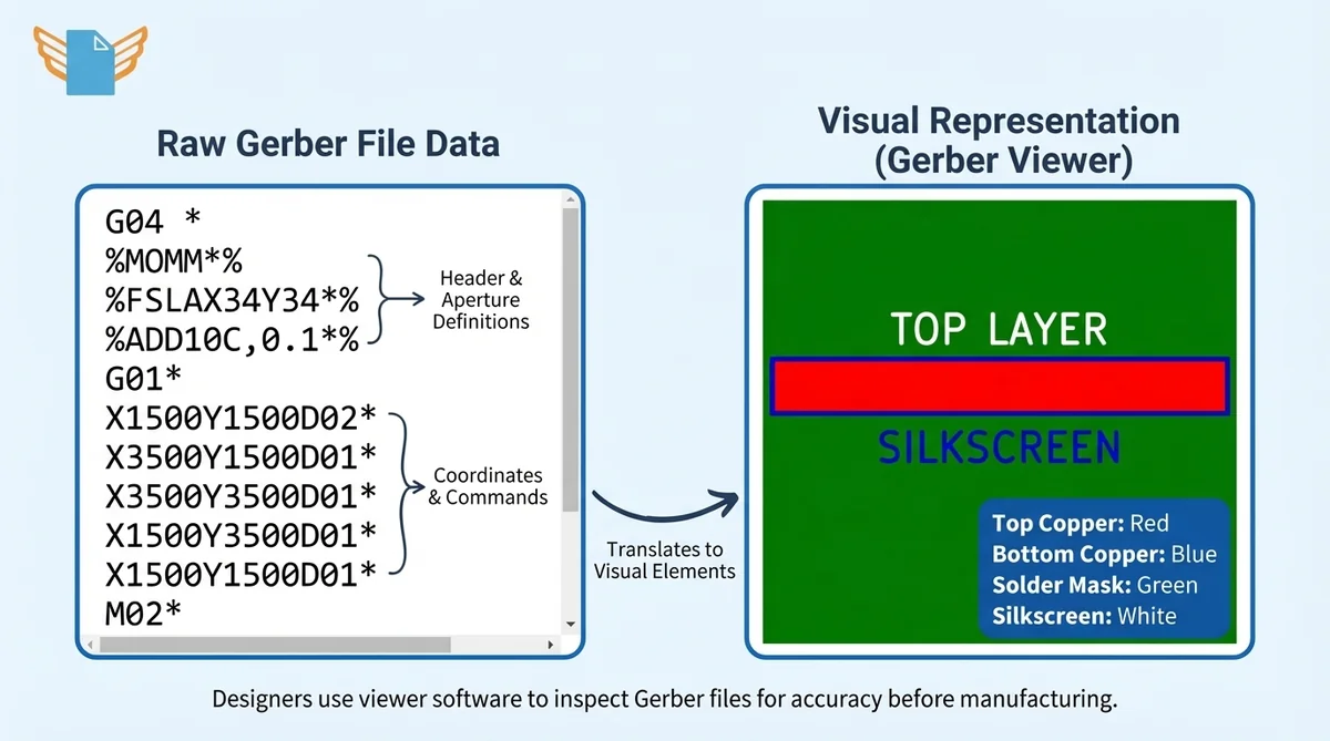
A Gerber file has two faces: raw text data and a rendered visual. Raw data appears as ASCII characters with coordinate pairs, aperture codes, and command sequences. A human can read portions in a text editor. However, interpreting the full board geometry from code alone is not practical.
Gerber viewer software translates raw commands into a visual PCB layer image. Tools such as KiCad’s GerbView, Ucamco’s Reference Gerber Viewer, and the open-source Gerbv display each layer using standard color conventions: top copper in red, bottom copper in blue, solder mask in green, silkscreen in white. Gerber viewers run on Windows, Mac, Linux, and web browsers. Most viewers support both RS-274X and Gerber X2 file imports, including .gbr, .gtl, and .gbl extensions.
Design verification before sending files to a manufacturer is critical. KiCad provides a free built-in viewer. Ucamco publishes a free Reference Gerber Viewer for validating files against the official specification. Engineers should check these elements during inspection:
- Copper traces for continuity, width, and clearance
- Solder mask openings for alignment with copper pads
- Silkscreen text for readability and correct placement
- Board outline for accurate dimensions and shape
- Drill hole positions for alignment with pads
Essential Gerber File Layers for PCB Manufacturing
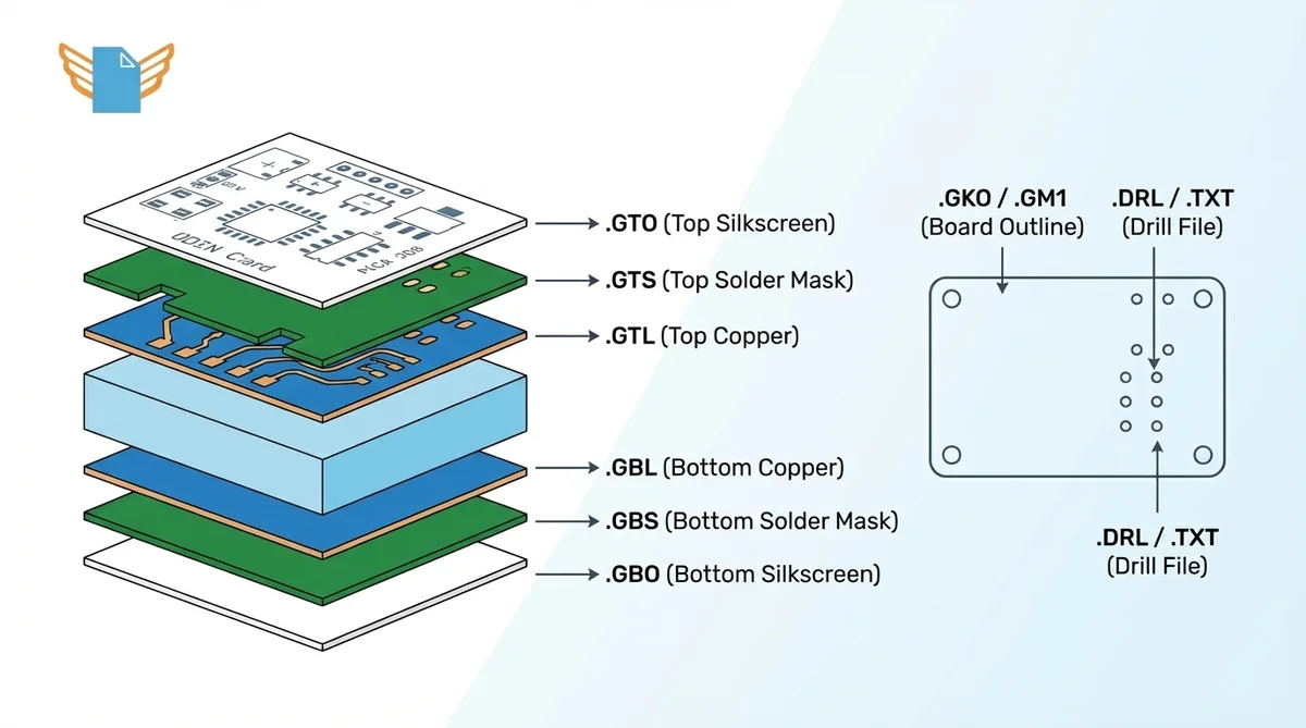
What Gerber files do you need? A complete file package for a two-layer PCB contains 7 to 8 individual files. Each file defines one physical layer or manufacturing instruction.
| Layer | Extension | Function |
|---|---|---|
| Top copper | .GTL | Copper traces, pads, and pour on top |
| Bottom copper | .GBL | Copper traces, pads, and pour on bottom |
| Top solder mask | .GTS | Solder mask coverage and openings on top |
| Bottom solder mask | .GBS | Solder mask coverage and openings on bottom |
| Top silkscreen | .GTO | Component labels, outlines, markings |
| Bottom silkscreen | .GBO | Bottom-side labels and markings |
| Board outline | .GKO / .GM1 | Physical dimensions and cut path |
| Drill file | .DRL / .TXT | Hole positions, sizes, types (Excellon format) |
Multilayer boards add inner copper layer files (.G2, .G3 for layers 2 and 3). Stencil production during assembly requires solder paste layers (.GTP, .GBP). The layer stacking order runs from top to bottom. That order matches the physical structure of the finished board.
Before submitting, designers should compress all Gerber files, drill files, and a readme into one ZIP archive. Following the fabricator’s naming guidelines prevents misinterpretation.
Frequently Asked Questions
What is a Gerber file?
A Gerber file is a vector-based 2D image format that transfers PCB design data to manufacturers. The Gerber format uses ASCII commands to describe copper traces, solder mask geometry, silkscreen markings, and board outlines for each layer.
What is the purpose of Gerber files?
Gerber files serve as fabrication instructions for PCB manufacturing equipment. The format tells machines where to etch copper, apply solder mask, print silkscreen, and drill holes. Every fabrication house worldwide accepts Gerber data.
Why are Gerber files required?
PCB manufacturers cannot read native design files from EDA tools like Altium Designer or KiCad. Gerber files provide a standardized, software-independent format. The Gerber file format has been the de facto industry standard since the late 1990s.
What information is stored in a Gerber file?
Each Gerber file contains aperture definitions, coordinate data (XY positions), and draw/flash commands (D-codes and G-codes). The file defines one PCB layer at a time. A complete set covers copper, solder mask, silkscreen, board outline, and drill data.
What are the different Gerber file formats?
Three Gerber format versions exist: RS-274D (revoked in 2014), RS-274X (current standard), and Gerber X2 (latest, with embedded metadata). Ucamco recommends RS-274X as the minimum and X2 as the preferred choice.
Convert Gerber files online
Free, no installation, no upload limits — convert right in your browser: